


Smarter devices are often discussed in terms of software, artificial intelligence, and connectivity. Yet every connected product still depends on physical components that must fit, conduct, shield, filter, and move with precision. As software capabilities continue to expand through AI, edge computing, embedded systems, and the Internet of Things (IoT), hardware must evolve alongside them. The miniature metal components inside these systems play a critical role in ensuring reliable performance, signal integrity, and compact product designs. As products become smaller and more complex, manufacturers need methods that can create detailed metal parts without adding unnecessary stress or tooling cost. This is where photochemical etching services are becoming increasingly valuable in modern product development.
Table of contents
Miniaturization Creates New Manufacturing Challenges
Smaller devices are changing almost every industry. Wearables need thinner internal parts. Medical equipment needs compact components that work reliably, even in tough conditions. Electric vehicles pack in dense electronic systems. Robots and industrial sensors need accurate movement and feedback.
These products often use thin metal parts with narrow slots, small holes, repeated patterns, complex edges, or precise contact points. Even a small burr can interfere with assembly. Too much heat can warp a delicate part. Mechanical pressure can bend the part or introduce stress that affects performance.
Stamping, laser cutting, and CNC machining remain important manufacturing methods. However, they do not always suit thin, intricate components used in today’s connected electronics and embedded systems. Hard tooling can be expensive during product development, while thermal or mechanical cutting often requires additional finishing. As software-driven products become increasingly compact and feature-rich, engineers need manufacturing methods that support detailed geometries, rapid design iterations, and precision from prototype through production.
How Photochemical Etching Works
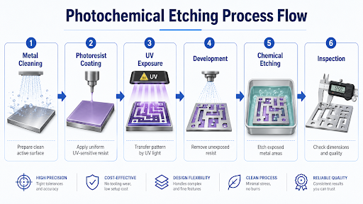
Photochemical etching is also called photo etching or photochemical machining. It removes metal from a sheet using a controlled chemical process rather than a cutting tool.
Here’s how it works:
- A metal sheet is cleaned and coated with a light-sensitive coating called photoresist.
- Digital artwork with the part’s design is transferred onto the sheet using UV light.
- The protected areas stay covered, while a chemical called an etchant removes the exposed metal.
- The finished parts are cleaned and inspected.
Since no cutting tool is used, the process avoids applying mechanical force to the part. It can also create holes, slots, tabs, grids, identification marks, and fold lines on the same sheet.
Digital artwork also makes design changes simple. Engineers can update a design without ordering new hard tooling for every revision. This flexibility supports rapid prototyping, testing, and low- to medium-volume production, helping technology companies accelerate hardware development alongside evolving software and electronic system requirements. According to McKinsey, organizations using digital product development approaches such as digital twins have reduced product development times by 20% to 50% while lowering costs and reducing the number of physical prototypes required.
Why the Process Fits Modern Product Development
Photochemical etching is most useful when a component is thin, geometrically complex, or sensitive to conventional cutting.
One advantage is edge quality. The process can produce parts without the raised burrs often created by mechanical blanking. This reduces the need for deburring and lowers the risk of sharp edges affecting assembly or electrical performance.
Another advantage is feature density. Hundreds of holes or repeated patterns can be etched simultaneously instead of being cut individually. This is especially valuable for screens, encoder disks, apertures, shielding components, and fine grids used in advanced electronic systems.
The process can be applied to stainless steel, copper alloys, nickel alloys, and other sheet metals. Material selection depends on electrical conductivity, corrosion resistance, mechanical strength, and forming requirements.
Product teams evaluating this manufacturing method can learn more about TMNetch’s custom photo etching services, including support for prototypes and custom precision metal components.
Where Etched Components Support Smart Technology
Electronics and Connected Devices
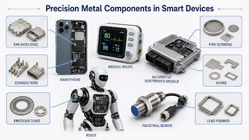
Smart electronics contain many hidden metal components. EMI and RFI shielding covers protect sensitive circuits from interference. Lead frames connect semiconductor chips. Contacts and connectors carry power or signals. Fine screens support airflow, filtration, or protection.
As devices become thinner, these components require tighter packaging and increasingly detailed geometries. Etching can create openings, tabs, bend lines, and identification features on a single flat piece before it is formed into its final shape. These precision components also help embedded software, processors, communication modules, and wireless systems operate reliably by maintaining signal integrity and electromagnetic compatibility.
Medical Technology
Medical devices often require miniature components for diagnostics, sensors, fluid control, filtering, positioning, and electronic protection. Examples include encoder disks, contact elements, fine meshes, shielding parts, and precision shims.
Consistent dimensions and clean edges are especially important in healthcare applications. As medical technology increasingly incorporates embedded software, AI-assisted diagnostics, and connected patient monitoring, precision hardware becomes equally important. Choosing the appropriate manufacturing method also requires evaluating material compatibility, cleaning requirements, regulatory standards, and product validation.
Mobility and Electric Vehicles
Modern software-defined vehicles rely on growing numbers of sensors, electronic control units, communication modules, and power-management systems. Etched parts are commonly used in shielding cans, battery-related components, encoder elements, flat springs, contacts, filters, and spacers.
Photochemical etching is particularly valuable when designs combine thin materials with numerous fine features or require frequent revisions during product development. These precision components support the electronic systems that enable advanced driver assistance, vehicle connectivity, battery management, and future mobility technologies.
Robotics and Industrial Automation
Robots, motion systems, industrial sensors, and Industry 4.0 equipment depend on accurate feedback and compact assemblies. Photochemical etching can produce encoder disks, apertures, shims, springs, and sensor-related components suitable for flat-sheet manufacturing.
Although these parts are physically small, they play an important role in alignment, motion accuracy, signal quality, and overall system reliability. They also support robotic systems that rely on software for motion control, machine vision, real-time monitoring, and intelligent automation.
When Should Engineers Consider Photochemical Etching?
Photochemical etching should be considered when a part:
- Is made from thin metal sheet or foil.
- Contains complex internal openings or repeated patterns.
- Requires clean edges with minimal mechanical stress.
- May go through several design revisions.
- Needs to move from prototype to repeat production.
- Includes tabs, slots, fold lines, or identification marks in one flat pattern.
It is not the best choice for every application. Thick, highly three-dimensional parts may be better suited to CNC machining. Simple parts produced in very high volumes may justify stamping tools. Some thicker flat parts may be more economical to laser cut.
The best manufacturing decision comes from comparing geometry, material, tolerances, thickness, production volume, secondary operations, and total project cost.
While software enables intelligence, analytics, automation, and connectivity, these capabilities ultimately depend on hardware that performs reliably in demanding environments. Precision-manufactured metal components help ensure that sensors, communication modules, processors, shielding systems, and embedded electronics function consistently across today’s connected technologies. Manufacturing methods such as photochemical etching therefore play an important supporting role in the broader technology ecosystem.
The Hardware Layer Behind Emerging Technology
The most visible advances in technology may happen in software, artificial intelligence, and data, but smart products still depend on precisely manufactured hardware. Shielding parts, contacts, encoder disks, fine screens, lead frames, and shims allow devices to connect, sense, communicate, and operate reliably.
By supporting detailed geometries, thin materials, and flexible design changes, photochemical etching gives product teams another way to develop the precision-etched electronic components used inside modern devices.
As AI, IoT, robotics, edge computing, and embedded systems continue to evolve, manufacturing methods that enable compact and highly reliable electronic hardware will become even more important. Better products will depend not only on faster processors and smarter software, but also on the precision-engineered metal components that make those technologies possible.