
In the intricate world of printed circuit board (PCB) design, few parameters hold as much sway over a board’s performance, reliability, and safety as PCB trace width. Often appearing as a minor setting in layout software, the width of these tiny copper paths is a monumental decision, directly impacting everything from current handling capacity and thermal management to signal integrity in high-speed applications. An incorrectly sized trace can transform a sophisticated circuit into a melted fuse or an unreliable data link.
This comprehensive guide will demystify PCB trace width, delving into its fundamental importance, the critical factors that dictate its size, the industry-standard calculations (including IPC standards), and best practices for optimizing your designs. Whether you’re working on high-power distribution or delicate high-speed circuits, mastering trace width is your gateway to professional-grade PCB engineering.
Key Takeaways
- Incorrect PCB trace width is a common cause of board failure, leading to overheating or signal issues.
- Key factors influencing trace width include current, copper weight, allowed temperature rise, and layer placement.
- IPC-2221 provides general trace width calculations, while IPC-2152 offers more precise thermal modeling.
- Always use a trace width calculator and incorporate safety margins into your designs.
- For high-speed designs, maintain consistent trace widths and utilize reference planes for controlled impedance and signal integrity.
- Wider traces are generally better for power but must be balanced with routing density and signal impedance requirements.
Table of contents
What is PCB Trace Width and Why Does It Matter?
At its core, PCB trace width refers to the physical width of the copper conductor connecting components on a printed circuit board. These traces are the electrical arteries of your board, carrying current and signals between various points. While seemingly simple, their dimensions are paramount.
The significance of trace width stems from several critical electrical and physical phenomena:
- Current Carrying Capacity: Every trace has electrical resistance. When current flows through this resistance, it generates heat, a phenomenon described by Joule’s Law (P = I²R). If a trace is too narrow for the current it carries, its resistance will be higher, leading to excessive heat generation. This can cause the trace to overheat, delaminate, melt, or even act as an unintended fuse, leading to catastrophic board failure or fire. Proper trace width ensures the board can safely handle the required current capacity without thermal stress.
- Temperature Rise: Directly linked to current capacity, the trace width dictates how much the trace’s temperature will rise above ambient. Designers must ensure this temperature rise remains within safe operating limits for the board materials and surrounding components.
- Signal Integrity: For high-speed circuits and RF applications, trace width is a crucial factor in maintaining consistent impedance, which is vital for preserving signal integrity. Variations in width can cause reflections and signal degradation, leading to unreliable data transmission.
- Voltage Drop: A narrower trace has higher resistance, leading to a greater voltage drop along its length, especially for power traces. This can starve components of their required voltage, impacting performance.
In essence, neglecting trace width is a common root cause of PCB failures, making its accurate calculation and thoughtful design indispensable for any reliable electronic product.
Key Factors Influencing Trace Width Design
Designing optimal trace widths isn’t a one-size-fits-all endeavor. Several interconnected factors must be considered:
Current (Amperage)
The most significant factor is the maximum continuous current a trace is expected to carry. Higher currents demand wider traces to minimize resistance and heat generation. Always account for peak currents and add a safety margin to prevent thermal runaway.
Copper Weight (Thickness)
Copper weight refers to the thickness of the copper foil on the PCB, typically measured in ounces per square foot (oz/ft²). Common values include 0.5 oz, 1 oz, 2 oz, and sometimes higher for power applications. A thicker copper layer (higher oz value) offers lower resistance for a given trace width, allowing it to carry more current or a narrower trace to be used for the same current. The standard assumption for many calculations is 1 oz copper (approximately 1.378 mils or 35 µm thick).
Permissible Temperature Rise
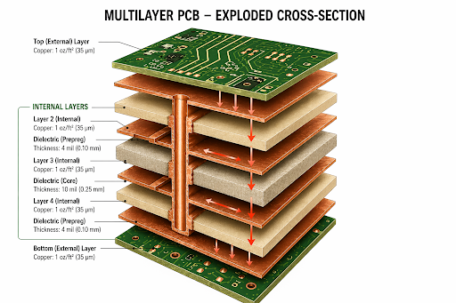
This is the maximum allowable temperature increase of the trace above the ambient temperature of the board. This value is critical because exceeding it can degrade PCB materials, stress components, and reduce the overall lifespan of the board. Typical temperature rise limits range from 10°C to 20°C for general applications, but can be lower for sensitive circuits. 3.4. Layer Placement (Internal vs. External Layers)
Traces on internal layers of a multilayer PCB dissipate heat less efficiently than those on external layers. External layers benefit from convection cooling from the surrounding air and radiation. Consequently, an internal trace generally needs to be significantly wider than an external trace to carry the same current and achieve the same temperature rise. This distinction is crucial for proper power distribution.
Ambient Temperature
The operating environment’s maximum temperature influences how much additional heat the traces can safely generate. A board operating in a hot enclosure will have less thermal headroom than one in a cool, well-ventilated area.
| Factor | Impact on Trace Width | Notes |
|---|---|---|
| Current | Higher current = Wider trace | Most significant factor; dictates heat generation. |
| Copper Weight | Thicker copper = Narrower trace for same current | Typically 1oz, 2oz, 3oz; measured in oz/ft ². |
| Temperature Rise | Lower allowed rise = Wider trace | Critical for material integrity & component reliability. |
| Layer Placement | Internal trace = Wider than external for same current | External layers dissipate heat more effectively. |
| Ambient Temp. | Higher ambient = Wider trace needed (less thermal margin) | Consider operating environment. |
IPC Standards: Your Guiding Principles
For professional and reliable PCB design, adhering to industry standards is non-negotiable. Two primary IPC standards govern trace width calculations:
IPC-2221 (Generic Standard on Printed Board Design)
This is the classic, more general standard. IPC-2221 provides empirically derived charts and formulas that relate trace width, copper weight, current, and temperature rise. It’s widely used for most general-purpose PCB designs. The formulas within IPC-2221 distinguish between internal and external layers due to differing thermal characteristics.
The core formulas for calculating trace width based on IPC-2221 are as follows:
First, the Area is calculated:
Area[mils²] = (Current[Amps]/(k*(Temp_Rise[deg. C])^b))^(1/c)
Then, the Width is calculated:
Width[mils] = Area[mils²]/(Thickness[oz]*1.378[mils/oz])
Where k, b, and c are constants:
- For IPC-2221 internal layers: k = 0.024, b = 0.44, c = 0.725
- For IPC-222 1 external layers: k = 0.048, b = 0.44, c = 0.725
These constants are derived from curve fitting to the IPC-2 221 graphs.
IPC-2152 (Standard for Determining Current-Carrying Capacity of Conductors in Printed Boards)
IPC-2152 is a newer, more comprehensive standard that offers more precise calculations, especially for varying board materials, thermal conductivity, and environmental factors. It addresses some limitations of IPC-2221 by considering heat dissipation more holistically, including adjacent traces and planes. While more complex to apply manually, it provides more accurate results for high-reliability or thermally sensitive designs. Many advanced trace width calculator tools use IPC-2152 for enhanced precision.
For most designers, starting with IPC-2221 is sufficient, but understanding the existence and benefits of IPC-2152 is key for advanced applications.
Calculating Trace Width: Formulas and Tools
Manually calculating trace widths using the IPC formulas can be tedious. Fortunately, numerous PCB manufacturers offer online calculators that can greatly simplify this process. These calculators typically require inputs such as:
- Maximum Current (Amps)
- Copper Weight (oz)
- Desired Temperature Rise (°C)
- Layer Type (Internal or External)
Some calculators also allow for optional inputs like ambient temperature or trace length, which can influence voltage drop. Always use a reputable calculator that explicitly states its adherence to IPC standards.
A good practice is to input your design parameters and compare results from different calculators or cross-reference with IPC tables to ensure consistency. Remember that these calculations provide estimates; always add a safety margin to your final trace widths to account for manufacturing variations and unforeseen thermal stresses.
Best Practices for High-Performance Designs
Beyond basic calculations, optimizing trace width for specific applications requires strategic thinking:
High-Current and Power Distribution
- Generous Widths: For power rails, err on the side of wider traces. This minimizes voltage drop and reduces heat, improving overall system efficiency and reliability.
- Thermal Relief Pads: When connecting large power traces to component pads, use thermal relief patterns to ensure proper soldering.
- Copper Pours and Planes: Utilize copper pours or dedicated power and ground planes for significant current distribution. These act as extremely wide traces, offering superior current capacity and heat dissipation.
- Multiple Traces: For very high currents, consider routing multiple parallel traces to share the load.
High-Speed and RF Circuits
For these applications, signal integrity is paramount, and trace width is directly tied to characteristic impedance.
- Controlled Impedance: Design traces to a specific characteristic impedance (e.g., 50 Ohm or 75 Ohm) to prevent reflections. This often requires precise control over trace width, dielectric thickness, and ground plane proximity.
- Consistent Widths: Maintain uniform trace widths along the entire length of a high-speed signal path to avoid impedance discontinuities.
- Reference Planes: Always provide a continuous reference plane (ground or power) adjacent to high-speed traces. This is crucial for defining impedance and returning currents.
- Differential Pairs: For differential signals, ensure the two traces in the pair have identical widths and spacing to maintain common-mode rejection and impedance control.
General PCB Design Tips
- Design Rules: Configure your PCB design software’s design rules to automatically check minimum trace widths based on your current requirements and IPC guidelines.
- Clearance: Ensure adequate spacing between traces ( and between traces and pads/vias) to prevent short circuits and meet manufacturing tolerances, especially when using wider traces.
- Routing Density: Balance trace width with routing density. While wider is generally better for current, extremely wide traces can consume valuable board space, making routing complex.
- Documentation: Clearly document your trace width decisions, especially for critical power and signal paths, including the reasoning (e.g., “30 mil trace for 2 A @ 10°C rise, external layer, 1oz copper”).
FAQ
Question1: What is the difference between IPC-2221 and IPC-215 2?
Answer: IPC-2221 is a classic, general standard based on empirical data for basic trace width calculations. IPC-2152 is a newer, more precise standard that considers more complex thermal factors and board materials, offering more accurate results for demanding applications.
Question2: Why do internal traces need to be wider than external traces for the same current?
Answer: Internal traces are surrounded by dielectric material, which inhibits heat dissipation. External traces benefit from convection cooling from the air and radiation, allowing them to carry the same current with less temperature rise for a given width.
Question3: Can I just use the widest possible trace for everything?
Answer: While wider traces generally mean lower resistance and better current capacity, excessively wide traces consume valuable board space, increasing board size and cost, and potentially complicating routing for other signals. For high-speed signals, impedance matching dictates specific widths, not just “widest possible.”
Question4: What is “copper weight” in PCB design?
Answer: Copper weight refers to the thickness of the copper layer on the PCB, measured in ounces per square foot. A higher copper weight (e.g., 2 oz vs. 1 oz) means a thicker copper layer, which can carry more current for a given trace width.
Summary
Mastering PCB trace width is a cornerstone of robust and reliable electronic product development. From ensuring adequate current capacity and managing temperature rise to preserving signal integrity in demanding applications, the dimensions of your copper traces are paramount. By understanding the interplay of current, copper weight, allowed temperature rise, and layer placement, and by diligently applying IPC standards (IPC-2221 and IPC-2152), designers can prevent common PCB failures. Leveraging a reliable trace width calculator and adhering to best practices for power distribution and high-speed circuits will elevate your PCB design from functional to exemplary. Always prioritize safety margins and meticulous validation to achieve optimal performance and longevity for your printed circuit board.


