
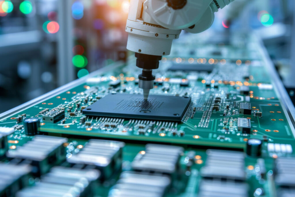
Modern technology relies on the steady progression of highly controlled manufacturing processes. The smartphones, AI systems, electric vehicles, medical devices, data centers, and connected devices you interact with daily all depend on chips that are continually becoming smaller, faster, and more efficient. Behind these advances are highly controlled manufacturing processes, and one of the most important is thin film deposition.
Building advanced electronics is not just about architectural design; it is about physically constructing billions of microscopic components with exceptional precision. By controlling how materials are layered on a substrate, engineers directly influence baseline chip performance and long-term structural reliability. Understanding how these microscopic layers are applied helps explain how the industry continues to improve device density, performance, and reliability. In this article, you will learn how the mechanics of layered material applications work and why they form the backbone of future technology.
Key Takeaways
- Thin film deposition adds extremely thin layers of material to semiconductors, crucial for modern chip manufacturing.
- Methods like Physical Vapor Deposition (PVD), Chemical Vapor Deposition (CVD), and Atomic Layer Deposition (ALD) are essential for precision.
- Material purity significantly affects thin film performance, impacting yield and device reliability.
- Thin films enable smaller, faster, and more efficient chips by improving transistor density and signal control.
- Future semiconductor advancements will rely on tighter tolerances, advanced chip architectures, and enhanced process control.
Table of contents
- What Is Thin Film Deposition?
- Why Thin Film Deposition Matters in Semiconductor Manufacturing
- Common Thin Film Deposition Methods Used in Chip Manufacturing
- Why Material Purity Matters in Thin Film Deposition
- How Thin Films Help Create Smaller, Faster, and More Efficient Chips
- Thin Film Deposition and the Future of Semiconductor Technology
- Key Challenges Manufacturers Still Need to Solve
- Final Thoughts
What Is Thin Film Deposition?
To understand how modern processors are built, you must first understand thin film deposition. At its core, it is the process of adding extremely thin layers of material onto a surface, usually a bare semiconductor wafer or substrate.
These layers are incredibly small—often measuring only a few nanometers or micrometers thick. Despite their diminutive size, these microscopic coatings fundamentally alter the behavior of the targeted underlying substrate. Depending on the material used, they can change the electrical, optical, protective, or mechanical properties of a surface to meet strict engineering requirements.
In practice, semiconductor devices are not created in a single isolated step. Instead, they are built through dozens of sequential layers and intricate microscopic patterning steps. Together, these carefully stacked and etched layers dictate how electricity flows, helping chips perform highly specific functions within a broader integrated circuit layout.
Why Thin Film Deposition Matters in Semiconductor Manufacturing
The true complexity of semiconductor thin film deposition lies in precise material placement. Semiconductor innovation is not only about high-level conceptual chip design; it depends entirely on the ability to place the exact right material in the exact right location with extreme precision.
Different layers serve highly specialized purposes within a functional microchip. First, they deposit targeted conductive layers to help create vital electrical pathways, ensuring logic signals travel efficiently across the device. Next, they apply dense insulating layers to shield active components and help prevent unwanted current flow between densely packed transistors.
Additionally, manufacturers apply tight barrier layers to help protect vulnerable sensitive materials from harsh chemical reactions during subsequent fabrication phases. Finally, they integrat protective coatings to improve the overall reliability and durability of the processor. Ultimately, these incredibly precise layers consistently help support smaller and correspondingly more complex modern chip designs.
Common Thin Film Deposition Methods Used in Chip Manufacturing
Semiconductor manufacturers use different deposition methods depending on the specific material profile, the internal device design, and the strict performance requirements of the final product.
Physical Vapor Deposition
Physical vapor deposition, commonly known as PVD, is a purely physical transfer process. It involves vaporizing a solid source material in a sealed vacuum chamber and forcefully depositing it as a thin film on the wafer surface. Because it does not rely on complex chemical reactions on the substrate, it remains highly predictable. PVD is often used by fabrication lines for placing stable metal layers, highly conductive films, and specialty protective coatings.
Chemical Vapor Deposition
Unlike PVD, chemical vapor deposition (CVD) relies entirely on integrated chemical interactions. CVD uses tightly controlled gas-phase chemical reactions to form a dense solid film directly on the wafer surface. The precursors interact upon entering the heated chamber, leaving behind the desired structural coating. CVD is widely used throughout the industry for applying heavy dielectric layers, fundamental silicon-based films, and various other essential semiconductor materials.
Atomic Layer Deposition
When manufacturers require exceptionally precise structural control, atomic layer deposition (ALD) serves as the primary method. ALD uses sequential, self-limiting surface reactions to build films with atomic-scale thickness control, reliably providing very high physical precision. ALD is especially useful for fabricating complex modern chip structures where exceptionally uniform coverage over deep trenches is important.
Sputtering and Evaporation
These are two highly important PVD techniques. Sputtering uses introduced energetic particles, typically an inert gas plasma, to physically knock atoms free from a target source material. In contrast, evaporation systematically heats a raw source material until it vaporizes entirely inside the chamber. Once suspended, the resulting vapor then condenses directly on the bare wafer or substrate as an ultra-thin film. Both methods are important when manufacturers need tightly controlled material layers for optics, semiconductor applications, and complex electronics.
Why Material Purity Matters in Thin Film Deposition
Material quality plays a major role in thin film performance because even small inconsistencies can affect film uniformity, adhesion, conductivity, and long-term reliability. In evaporation-based PVD, the purity and consistency of the source material matter because the material is heated, vaporized, and condensed onto the substrate. For this reason, manufacturers often use high-purity evaporation materials to reduce contamination risk and improve repeatability. Choosing consistent source materials helps reduce contamination risks and supports repeatable deposition results across production runs.
Beyond the mechanical calibration of the primary deposition tools, the chemical integrity of the basic source elements heavily dictates the final factory output. Operating strictly with exceptionally high-purity materials ensures structural stability and actively helps reduce localized contamination within the sensitive vacuum chamber environment.
When external input variables are tightly managed, consistent source materials actively support highly repeatable daily deposition protocols batch after batch. Conversely, unexpectedly introducing poor material quality into the active production line can lead to structural defects, wildly uneven films across the substrate, or latent long-term electrical reliability problems. Because the margins for physical error are practically nonexistent at this scale, strict control over film quality directly affects total usable wafer yield, baseline processor performance, and overall manufacturing efficiency.
How Thin Films Help Create Smaller, Faster, and More Efficient Chips
The industrial demand for computationally heavy capability dictates the requirements of modern fabrication lines. Rigorous thin film deposition protocols actively support a broad array of critical modern chip improvements. By applying exceptionally uniform physical coatings, engineers can reliably fabricate smaller transistor structures and achieve a significantly higher core device density on a singular logic die.
These precise microscopic layers provide much better digital signal control and dramatically improved physical insulation between tightly grouped conductive lines. The net result of this precision is lower total power consumption and more efficient integrated chip performance.
Today, these targeted methods provide the required foundation to reliably support highly dense memory arrays, powerful micro-logic, responsive edge sensors, and advanced communication devices. These specific hardware components technically power real-world technology outcomes, making advanced AI chips, smartphones, rapid electric vehicles, massive cloud computing infrastructure, and localized smart devices possible.
Thin Film Deposition and the Future of Semiconductor Technology
As baseline hardware capability steadily escalates, thin film deposition will categorically become even more important as core semiconductor technology advances. The industry’s aggressive shift toward exceptionally advanced fundamental process nodes directly forces fabricators to maintain tighter structural tolerances.
Simultaneously, the widespread market adoption of vertical 3D chip architectures and highly advanced chiplet packaging requires flawless conformity. Fabricating highly specialized AI and heavy high-performance computing (HPC) chips inherently dictates the utilization of substantially more complex material stacks that naturally push current hardware limits.
To accommodate this, fabrication environments require much better real-time process monitoring and deeply integrated automated factory feedback limits. Future production lines will require greater atomic-scale precision, repeatability, and process control. Ultimately, future progressive semiconductor progress will fundamentally depend on the synthesis of two disciplines: ambitious architectural logic design and the flawless manufacturing precision required to construct those designs.
Key Challenges Manufacturers Still Need to Solve
While structural deposition mechanics are highly refined, fabrication facilities persistently face significant practical challenges that engineers still actively need to solve. A primary difficulty involves firmly maintaining highly uniform films on steadily smaller and more complex microscopic structural patterns.
At the extreme sub-nanoscale, trace molecular anomalies systematically cause failures, making the prevention of chemical contamination a relentless operational factory objective. Similarly, structurally controlling thin film thickness at remarkably small atomic scales requires perfect equipment calibration.
Process managers additionally struggle with simultaneously managing compounding commercial process costs while safely scaling highly advanced specialized deposition methods across mass volume runs. Furthermore, absolutely ensuring stringent quality consistency across continuous production environments introduces vast logistical variables. Facilities must continuously balance the difficult intersection of high line speed, molecular precision, and uncompromised wafer quality.
Final Thoughts
Thin film deposition fundamentally enables the next generation of advanced semiconductor manufacturing. As structural chips become smaller, noticeably faster, and highly complex, modern fabricators will definitively need substantially more precise deposition methods, strictly superior pure source materials, and drastically stronger operational process control. True technological hardware progress directly relies on expertly engineering reliable thin films at extreme microscopic scales.


